
| HOME |
Schematic |
Board Layout |
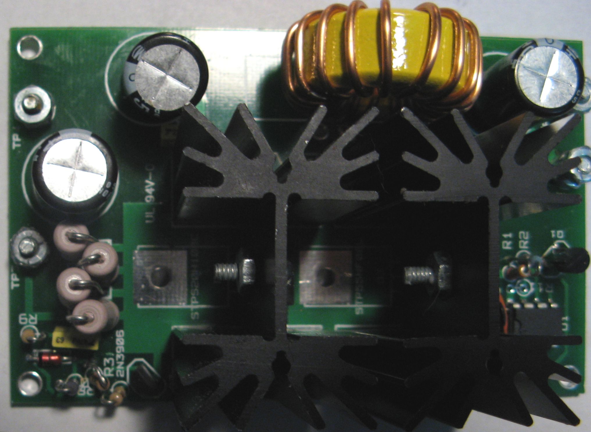
Board Photo-Large Heatsink |
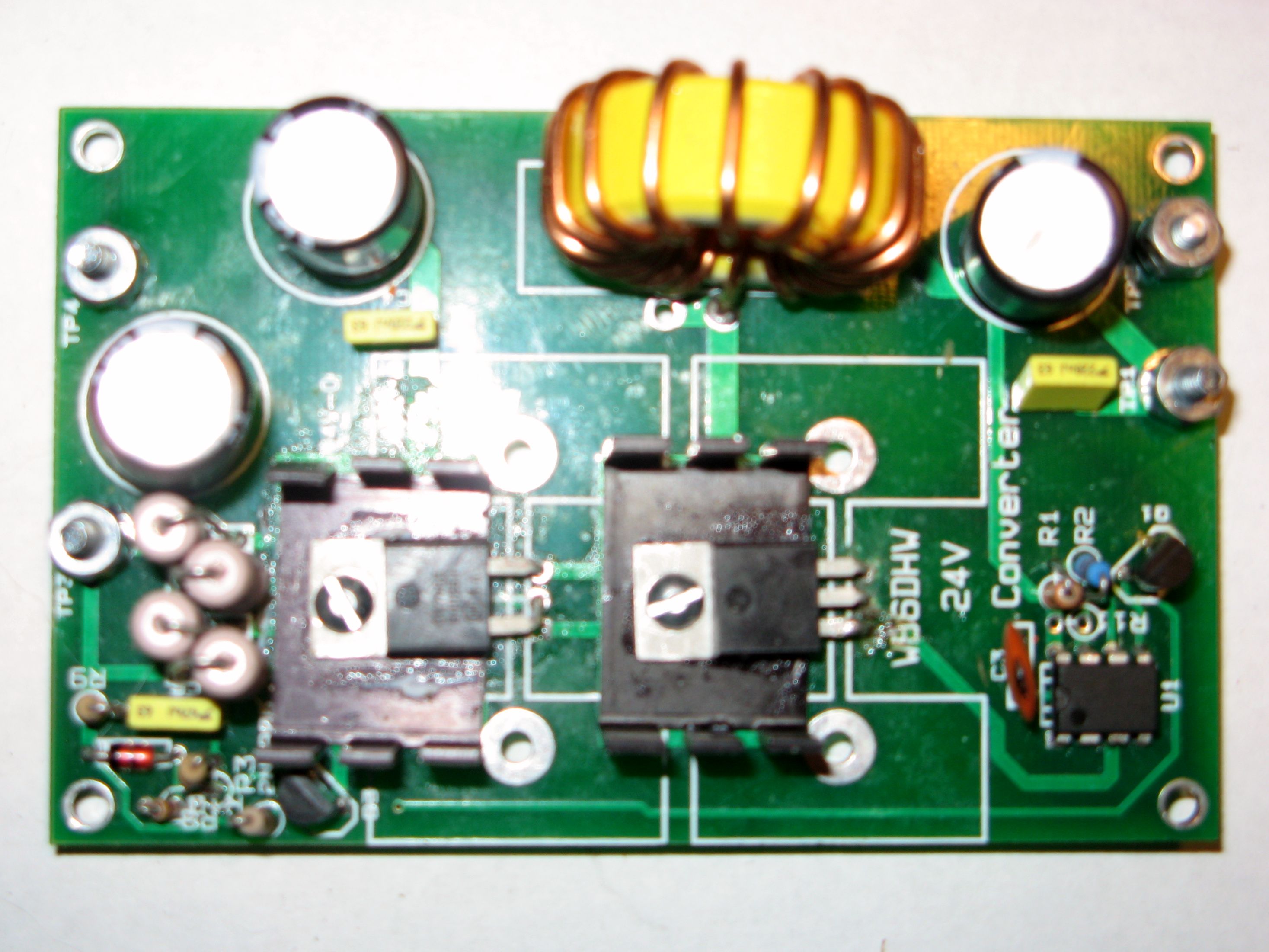
| Board Photo-Small Heatsink |
Parts List |
| E-Mail |
The circuit is a standard boost circuit switching regulator. U1(the NE555) provides a string of pulses at an approximate 50% duty cycly to control Q2, the MOSFET switch. With the switch off, the 12V input flows through the inductor, L1, and diode D1 to capacitors C4 and C4. C5 is for bulk storage and C4 is for RF filtering. When the output of the NE555 goes high, Q2 closes shunting the current from L1 to ground and causing the field to build up. When the NE555 output again goes low, the voltage across the coil will increase, trying to maintain the current flow. The higher voltage will charge C4 and C5 to a higher voltage than the supply voltage. Neglecting loses in D1 and Q2, C5 will charge to Vin X (1/(1-D)) where D is the duty cycle of the pulses. Thus for a Duty Cycle of .5(or 50%), the output is twice the input minus the losses in D1 and Q2. Q3, R3 to R7 form the current limit circuit. When the voltage drop across R4 to R7 exceeds the Emitter - Base voltage of Q3, Q1 will turn on and decrease the duty cycle or turn off Q2 altogether until the output current drops. D2, R10, and Q1 form the overvoltage circuit. If the output voltage rises above 24V, D2 conducts, turning on Q1 and reducing the NE555 output pulse duty cycle. The frequency and duty cycle of the NE555 are determined by R1, R2, R11 and C3. With R1 installed and R11 open, duty cycle is approximately 50%. By removing R1 and installing R11, duty cycle can be increased, increasing the output voltage. Note that D2 would also need increasing for higher voltage. The limiting factor on the output voltage obtainable is the voltage rating of Q2, D1, and C5. The maximum output obtainable is determined by L1, Q2 and D1 current ratings as well as the amount of energy L1 can store(Higher output currents may require more inductance to maintain output voltage ripple at an acceptable level). While the current limit circuit attempts to limit the current by reducing the output voltage, it can only reduce the output to the input voltage. Therefore, a fuse in series with the input should be used for absolute protecton of L1 and D1. |